What Are the Best Practices for Semiconductor Device Assembly?

Time:2026-08-31 Author:Aria
0%

The field of Semiconductor Device Assembly is critical in today's tech-driven world. As demand for high-performance electronic devices surges, industry practices must evolve. According to the latest SEMI report, the global semiconductor assembly market is projected to reach $50 billion by 2025. This growth underscores the importance of efficient assembly techniques.

Expert Dr. Alice Chen, a leading figure in semiconductor technology, asserts, "The quality of assembly processes directly impacts device performance and reliability." Her words highlight the need for best practices in assembly. These practices include rigorous quality control, advanced bonding techniques, and the adoption of automation.

In an industry where precision is key, even small errors can lead to significant failures. Companies must continually assess their assembly methods. This self-reflection is crucial for innovation. Despite advancements, occasional missteps in processes remind us of the importance of ongoing improvement. Ultimately, mastering Semiconductor Device Assembly will define the future of technology.
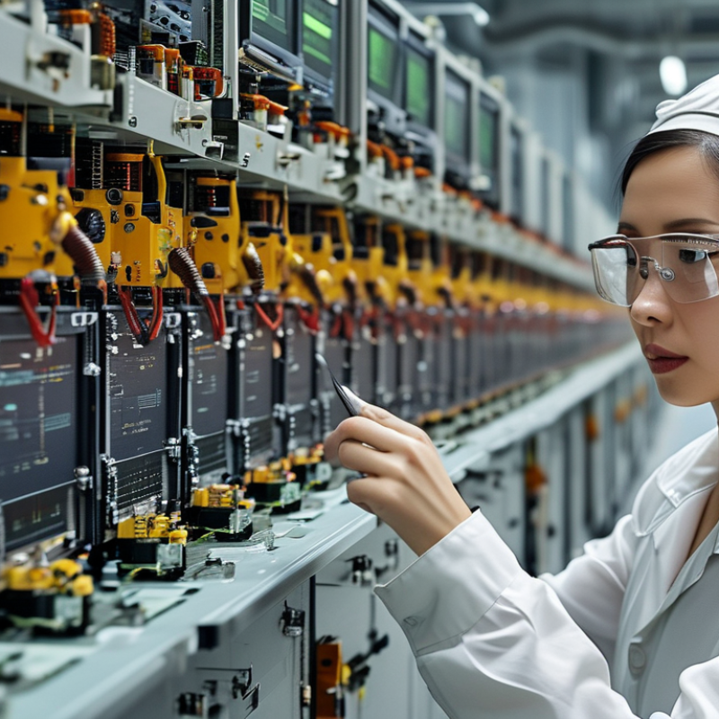
What Are the Best Practices for Semiconductor Device Assembly?

Overview of Semiconductor Device Assembly Processes

Semiconductor device assembly is a complex and critical process in electronics manufacturing. It requires precision and attention to detail. Each step plays a pivotal role in ensuring device performance and reliability. Common processes include die bonding, wire bonding, and encapsulation. These must be executed with strict control over environmental conditions.

Die bonding involves attaching the semiconductor die to a substrate. This step requires precise placement. Often, adhesive materials are used that can handle thermal and mechanical stress. Wire bonding then connects the chip to its package using fine wires. This requires expert handling to avoid damage. The encapsulation phase protects the device from environmental factors. Materials must be selected carefully to avoid compromising performance.

Challenges arise throughout these processes. Variation in materials and techniques can impact device quality. Continuous training for assembly technicians is essential. Regular equipment maintenance ensures consistent results. A robust quality control system is vital to catch potential failures early. By addressing these challenges, manufacturers can improve the reliability of their semiconductor devices, ultimately meeting the demands of an evolving technology landscape.

Key Materials Used in Semiconductor Device Assembly

Key materials play a crucial role in semiconductor device assembly. One of the most essential materials is silicon, widely used for its excellent electrical properties. However, silicon alone is not always sufficient. Compounds like gallium arsenide are sometimes preferred for specific applications. They offer better performance, yet they come with higher processing costs. This disparity necessitates a careful evaluation of material selection based on the intended use.

Another key material is the substrate on which devices are built. Common substrates include silicon wafers and polyamide films. The choice significantly impacts the thermal and electrical performance of the final product. Using inappropriate substrates can lead to failures and reduced efficiency. Additionally, adhesive materials and encapsulants help protect devices from environmental factors. However, their compatibility with other materials is not always guaranteed. This can lead to unexpected results in the manufacturing process.

Lastly, soldering materials are vital for ensuring connections between different components. Lead-free solders have gained popularity due to environmental concerns. But they may not provide the same reliability as lead-based options. Manufacturers often face challenges with joint integrity and thermal fatigue. Each material has its own advantages and disadvantages, requiring careful consideration when designing semiconductor devices.

Critical Steps in Semiconductor Packaging Techniques

In semiconductor packaging, various steps ensure device reliability and performance. Properly selecting materials is crucial. The choice of substrate affects thermal conductivity and signal integrity. Epoxy materials used for bonding must withstand temperature fluctuations. Inadequate selections can lead to device failure.

Assembly techniques also play a vital role in performance. Die bonding requires precision. Each chip must align perfectly to function correctly. However, many manufacturers struggle with alignment accuracy. This issue can impact yield rates and overall quality. A lack of proper training or techniques can contribute to this downfall.

Finally, testing and inspection cannot be overlooked. Post-assembly inspections reveal defects that may lead to larger failures. Inconsistent testing protocols can hide serious reliability issues. Companies need to reassess their quality control measures regularly. Skipping these steps may result in costly recalls and damaged reputations.

Quality Control Measures in Semiconductor Assembly

Quality control is critical in semiconductor assembly. According to a report by the Semiconductor Industry Association, defects can increase production costs by 20% or more. Implementing robust quality control measures can mitigate these risks significantly.

One effective strategy involves regular audits of the assembly process. These audits check for compliance with industry standards and best practices. They should focus on identifying potential sources of error in handling, soldering, and testing. Data suggests that companies conducting frequent audits see a 30% reduction in defects. Training personnel in quality control techniques is equally essential. When workers understand quality benchmarks, they can better identify issues.

Moreover, utilizing advanced technologies like machine learning can enhance quality control. Predictive analytics help in spotting trends and potential failures before they occur. A study indicated that companies using these technologies reported a 15% increase in production efficiency. Yet, implementing such systems can be challenging and resource-intensive. It requires a cultural shift within the organization, emphasizing quality over quantity. While technology can assist, human oversight remains indispensable.

Quality Control Measures in Semiconductor Assembly

Emerging Technologies and Trends in Device Assembly

As the semiconductor industry continues to evolve, new technologies are shaping device assembly processes. Automation is becoming more prevalent, reducing human error and increasing efficiency. Robots can handle complex tasks with precision, minimizing defects during assembly. However, reliance on automation raises questions about flexibility and adaptability.

Advanced packaging techniques are on the rise. Technologies such as 3D packaging and fan-out wafer-level packaging enhance performance and reduce size. These methods allow for better thermal management and connectivity. Still, the adoption of these techniques can be complicated and requires a skilled workforce.

One important aspect is continuous learning and adaptation. The assembly landscape changes rapidly with new materials and methods. Investing in employee training is crucial. Equally important is fostering a culture of innovation. Encouraging teams to experiment with new ideas can lead to significant breakthroughs.

Maintaining an agile supply chain is vital, too. Disruptions can happen, and companies need to be prepared. Building relationships with multiple suppliers creates resilience. Always monitor industry trends to adapt quickly. These strategies are essential for navigating the complexities of semiconductor device assembly in an ever-changing landscape.

FAQS

: What are key materials in semiconductor device assembly?

: Essential materials include silicon, gallium arsenide, substrates, adhesives, and soldering materials.

Why is silicon preferred for semiconductor devices?

Silicon has excellent electrical properties, making it a reliable choice for various applications.

What challenges arise from using gallium arsenide?

While it offers superior performance, gallium arsenide has higher processing costs.

How does substrate choice affect semiconductor devices?

Substrate selection impacts thermal and electrical performance, influencing overall device efficiency.

What role do adhesive materials play in semiconductor assembly?

They protect devices from environmental factors, but compatibility issues can occur.

Why are lead-free solders becoming popular?

Environmental concerns drive the shift towards lead-free options, despite some reliability issues.

How can quality control improve semiconductor assembly?

Implementing audits and training helps reduce defects and enhances overall production efficiency.

What benefits do advanced technologies offer in quality control?

Machine learning and predictive analytics help identify trends and potential failures, improving outcomes.

What should companies be cautious about when adopting new technologies?

Implementing advanced systems can be resource-intensive and require a culture shift towards quality.

How important is human oversight in quality control?

Human oversight remains essential, even as technology assists in identifying issues and trends.

Conclusion

Semiconductor Device Assembly is a crucial process in the manufacturing of electronic devices. It involves a series of well-defined steps that begin with the selection of key materials, which can include substrates, bonding wires, and encapsulants. The assembly process encompasses various packaging techniques, each tailored to enhance device performance and reliability. Critical steps within these techniques ensure proper integration of the semiconductor die with its package, addressing requirements such as thermal management and electrical interconnections.

Quality control measures play an essential role in Semiconductor Device Assembly, ensuring that each assembled device meets stringent industry standards. As technology progresses, emerging trends such as advanced automation and novel materials are shaping the future of assembly practices, promising increased efficiency and reduced costs. Understanding these best practices is vital for manufacturers aiming to enhance their production capabilities and maintain competitive advantage in the fast-evolving semiconductor industry.


Aria

Aria

Aria is a dedicated marketing professional with a deep passion for innovative strategies and a keen understanding of our company's product offerings. With a wealth of experience in the industry, Aria excels at crafting engaging content that highlights the unique features and benefits of our......