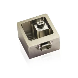
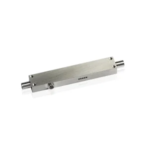
High-reliability processing accessories and hermetic seal components engineered for extreme environments
In the nano-scale world of contemporary sub-5nm semiconductor fabrication, the stability and cleanliness of wafer transport are paramount. **Semiconductor wafer handlers** function as the critical mechanical backbone of lithography, metrology, chemical-mechanical planarization (CMP), and etching tools. Any microscopic vibration, thermal variation, or particulate outgassing can disrupt chemical vapor deposition (CVD) or cause wafer breakage, resulting in millions of dollars of yield loss.
As a global frontrunner in advanced materials machining and micro-engineering, Xinyunyang Precision Technology Co., Ltd. addresses the industry's complex challenges by combining Kovar alloy processing expertise, micro-machined ceramic structures, and precision surface treatments. In wafer processing chambers that operate under extreme high-vacuum (UHV) and high-frequency RF fields (such as 40GHz networks), standard steel or aluminum components fail due to thermal expansion mismatch and high insertion loss.
Modern end-effectors require advanced structural design to balance weight-reduction and stiffness. We employ high-rigidity materials such as micron-level alloy steel tooling fixtures and aerospace safety armor designs to ensure that under high-speed lateral acceleration (up to 3G), the end-effector tip deflection remains below 10 micrometers. Eliminating vibration during transfer is the single most effective way to eliminate edge-chipping and backside scratch contamination on critical active layers.
Procurement specialists representing advanced fabrication units in North America, Europe, and East Asia operate under strict quality limits. Selecting a **semiconductor wafer handlers manufacturer** goes beyond simple piece-price economics; it demands strict adherence to rigorous quality frameworks, materials traceability, and absolute supply security.
Zero porosity in Kovar and precision ceramic components prevents moisture and gas trapping in extreme high vacuum environments.
Strict tolerances down to ±1 micrometer ensure high machine interchangeability across global manufacturing plants.
Gold plated surfaces, cleanroom-safe passivation, and anti-static coatings eliminate electrostatic discharge (ESD) incidents.
Xinyunyang meets these high standards by implementing strict trace-element testing on our raw materials. Whether dealing with high-purity Kovar alloy formulations for RF packages or micron-level alloy steel tooling fixtures, we verify structural uniformity through advanced metallographic analysis. This rigorous quality control ensures that our parts withstand high mechanical fatigue over millions of operational cycles.
The Chinese manufacturing ecosystem, specifically concentrated in the Pearl River Delta industrial corridor, offers distinct speed, cost-effectiveness, and vertical integration advantages. Xinyunyang Precision Technology Co., Ltd., founded in **November 2014**, has capitalized on this highly integrated network to build a vertically optimized supply chain.
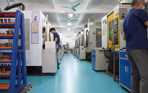
Unlike fragmented manufacturers who outsource plating, precision EDM, and heat treatment to third parties, Xinyunyang keeps all critical manufacturing processes in-house. Our advanced facility integrates raw material stock preparation, five-axis CNC precision machining, precision gold-plating, vacuum brazing, and ultimate cleanroom testing within a single unified workspace.
This unified operational control delivers a **15% to 20% improvement in delivery timelines** for critical components compared to traditional Western supply channels. Furthermore, it enables flexible customization for low-volume, high-complexity R&D prototypes without requiring prohibitive setup charges. This capability makes Xinyunyang an invaluable partner for next-generation silicon photonics, RF communication systems, and customized hermetic package developments.
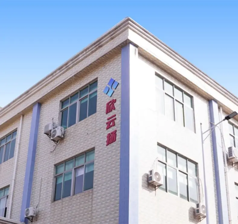
Xinyunyang Precision Technology Co., Ltd. is a leading advanced precision manufacturer founded in **November 2014**. From the beginning, the company has adhered to its initial focus on precision engineering, sticking to the business principles of **Integrity, Innovation, Cooperation, and Sharing**.
Our company focuses on Kovar precision processing technology as its core competitiveness. We deeply cultivate the fields of **semiconductors, optical communications, aerospace, medical devices, and the new energy/military industries**, and we are dedicated to providing miniaturized, customized, and high-reliability metal packaging solutions to global customers.
 High-precision processing capability Advanced technology and equipment Strict quality control Flexible customized services
The company maintains a professional team of more than 100 highly skilled personnel, with dedicated technical engineers accounting for 30% of our workforce.
Our core members have been deeply engaged in precision metal processing for over ten years, continuing to explore composite processing of special metals such as Kovar and titanium alloys, and proactively laying out cutting-edge packaging needs for 5G, AI, and new energy.
With our ISO 9001 certified quality management system and intelligent production scheduling system, Xinyunyang has increased regular order delivery efficiency by 15%-20%, serving as a key global partner with both technical depth and service breadth.
Operating in international semiconductor markets requires strict compliance with globally recognized standards. Our custom manufacturing processes align with the stringent demands of modern cleanroom equipment builders and device packaging facilities.
Our materials comply with crucial industrial and safety standards, including **SEMI S2 (Environmental, Health, and Safety Guidelines for Semiconductor Manufacturing Equipment)** and **SEMI S8 (Safety Guidelines for Ergonomics Engineering)**. This ensures that every high-quality wafer handler or end-effector we supply meets international safety criteria for integration into leading OEM platforms.
To support our clients in the Americas, Europe, and Asia, Xinyunyang offers comprehensive localization assistance, including complete material certifications (RoHS and REACH compliance reports), material test reports (MTR), and rapid-response technical consulting. We provide on-demand, customized support to quickly resolve technical queries regarding thermal expansion, material outgassing, and component dimensions.
Wafer handling components require tailored configurations based on the specific manufacturing step. Below are some key application scenarios where Xinyunyang's specialized products deliver exceptional performance:
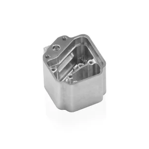
Under Extreme Ultraviolet (EUV) light conditions, any outgassing from volatile organic compounds or moisture instantly spoils expensive optical mirrors. Our ultra-high-density **Kovar alloy packaging lids** and high-precision CNC components undergo proprietary vacuum cleaning and bake-out steps. The resulting assemblies exhibit negligible outgassing rates, ensuring stable, reliable operation in high-vacuum environments.
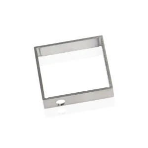
Thinned silicon wafers (under 100 micrometers thick) used for 3D TSV (Through-Silicon Via) stacks are highly fragile. Mechanical stress or uneven support can cause micro-fractures. We supply ultra-flat metal backing plates and support frames with flatness within 5 micrometers. This helps minimize structural stress and protects delicate wafers during transfer.
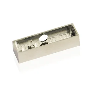
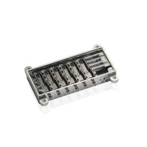
At frequencies up to 40GHz, standard packages suffer from signal distortion and high insertion loss. Xinyunyang manufactures **precision 5G Kovar alloy enclosures** that offer an insertion loss of under 0.26dB at 40GHz. This outstanding performance is made possible by our precise CNC machining and specialized plating technologies, which prevent electromagnetic interference and maintain high signal integrity.
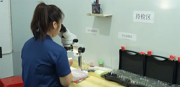
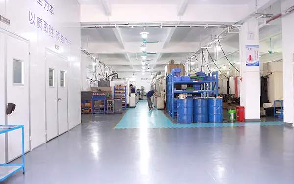
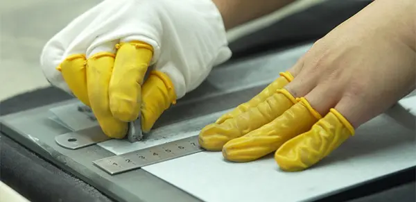
Inside Xinyunyang: High-accuracy CNC centers, testing zones, and our manufacturing workflow
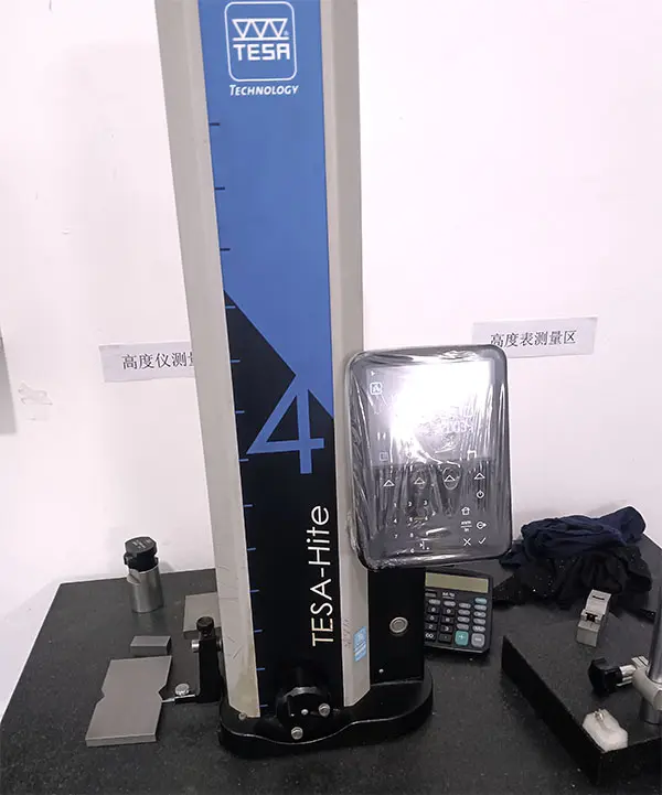
Our senior engineering and metallurgical specialists answer frequently asked questions regarding semiconductor wafer handling, thermal matching, and materials selection.
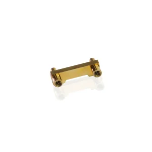
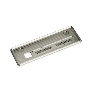
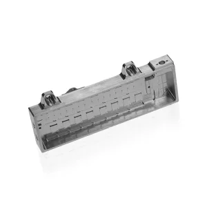
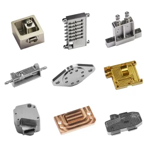
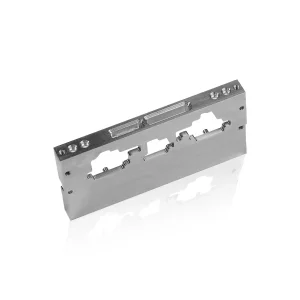
High-end industrial equipment panels, linear actuators, and micron-level tooling components
 Xinyunyang Precision