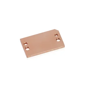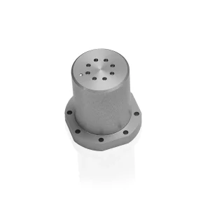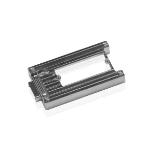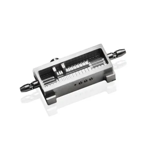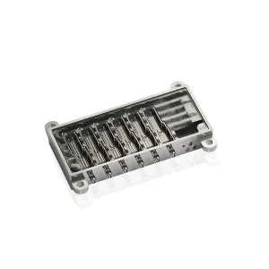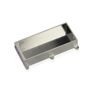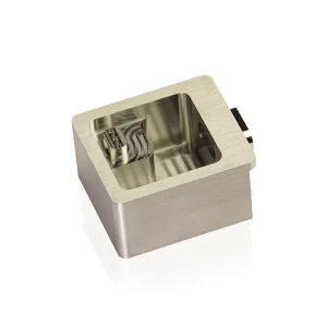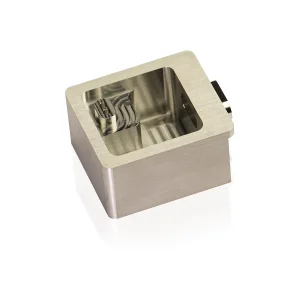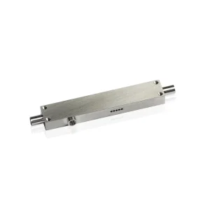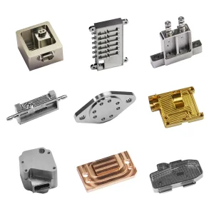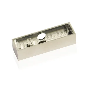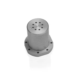
Founded in November 2014, Xinyunyang Precision Technology Co., Ltd. has steadfastly adhered to its initial intention of industrial excellence. Built upon the core business principles of Integrity, Innovation, Cooperation, and Sharing, we have earned a stellar reputation in the precision micro-manufacturing landscape.
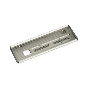
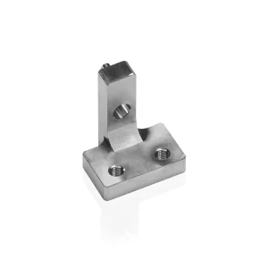
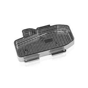
Our organization focuses on Kovar precision processing technology as its core competitiveness. We deeply cultivate critical application matrices across semiconductors, optical communications, aerospace, medical devices, and new energy or military industries. We are heavily committed to providing miniaturized, customized, and high-reliability metal packaging solutions to global customers. Our overarching goal is to remain a significant hermetic package lids, Kovar alloy components, and precision parts supplier in China and worldwide after years of rigorous, continuous efforts.
 High-Precision Processing
Advanced Tech & Equipment
Strict Quality Control
Flexible Customized Services
High-Precision Processing
Advanced Tech & Equipment
Strict Quality Control
Flexible Customized Services
The company boasts a highly trained professional team of more than 100 people, of which professional technical engineers account for over 30% of the entire workforce.
Our core members have been deeply engaged in precision metal processing for more than ten years. We proactively develop composite processing technologies for special alloys (Kovar, Titanium) to serve 5G, AI, and military aerospace demands.
Operating an ISO 9001 certified quality management ecosystem coupled with intelligent production scheduling, we have successfully optimized delivery efficiency for regular orders by 15% to 20%.
Kovar (ASTM F15, UNS K94610) is a nickel-iron-cobalt alloy engineered specifically for high-reliability hermetic sealing with borosilicate glass and ceramic materials. Our stamping methodology respects its complex metallurgical state.
The fundamental value of Kovar lies in its Coefficient of Thermal Expansion (CTE), which mimics the thermal curves of alumina ceramics and borosilicate glass (approximately 5.1 × 10⁻⁶/°C from 30°C to 400°C). When manufacturing components like hermetic lid packages or multi-lead headers, stampings must have zero micro-fractures. Any distortion in the grain structure during mechanical blanking or drawing can result in CTE deviation, causing seal failures at extreme high-temperature ranges.
Kovar is notoriously abrasive and undergoes rapid work hardening during progressive die stamping. At Xinyunyang, we employ controlled in-process intermediate annealing (usually in wet or dry hydrogen atmospheres at temperatures between 900°C to 1050°C). This ensures complete relief of mechanical stresses, recrystallization of the grain matrix, and decarburization of the surface, which is critically essential for bubble-free oxide formation during glass-to-metal sealing (GTMS).
| Chemical & Physical Properties of ASTM F15 (Kovar) | Composition / Value | Stamping & Engineering Impact |
|---|---|---|
| Nominal Composition | 29% Ni, 17% Co, Balance Fe | Strict metallurgical purity ensures consistent phase transitions down to -80°C. |
| Coefficient of Thermal Expansion (CTE) | 5.1 × 10⁻⁶/°C (30°C to 400°C) | Enables structural consistency with high-density alumina ceramics and borosilicate glass. |
| Tensile Strength (Annealed) | ≤ 550 MPa (approx. 75 ksi) | Low yield strength allows for highly detailed blanking, draw-forming, and embossing. |
| Thermal Conductivity | 17 W/m·K (at 20°C) | Requires active thermal management during high-speed precision stamping runs to preserve tooling. |
| Phase Stability | No transformation down to -196°C | Guarantees hermetic packaging integrity in deep space exploration and cryogenic environments. |
The rapid expansion of high-frequency communications, automated defense networks, and AI-optimized computing architectures has escalated the demand for hermetically sealed packaging components.
As data rates surge to 400G, 800G, and beyond, optical communication modules face immense thermal and electromagnetic challenges. Stamped Kovar baseplates, RF headers, and structural housings ensure minimal electrical signal loss while providing absolute protection against ambient moisture intrusion.
High-performance AI hardware relies on multi-chip architectures that require clean, ultra-flat structural lids. Our precision stamped Kovar lids protect high-value silicon dies from environmental stress while facilitating excellent heat dissipation via selective plating with nickel and gold.
Spaceflight equipment operates in harsh, extreme environments. Stamped Kovar alloys prevent outgassing, maintain absolute structural integrity under extreme G-forces, and resist phase transformation at ultra-low cryogenic temperatures encountered in vacuum conditions.
Xinyunyang ensures that our precision stamping services are strictly aligned with international industrial benchmarks and local environmental frameworks.
In today's integrated global supply chains, material traceability and environmental responsibility are paramount. We adhere to the strictest global frameworks, guaranteeing that our stamped parts are ready for seamless assembly anywhere in Europe, the Americas, and Asia.
To support high-growth global markets, Xinyunyang offers active design-for-manufacturing (DFM) consultancy directly to engineering teams. Whether you are scaling an initial prototype design in California, reviewing metallurgical tolerances in Munich, or setting up a high-volume manufacturing assembly line in Shenzhen, our engineering experts are available to consult on:
DFM Consultation Framework:
We provide precise die clearance engineering, progressive die strip layouts, and deep draw ratio calculation feedback within 48 hours. Our automated tooling design minimizes raw material waste by up to 18%, offering dramatic cost efficiencies at scale.
As microelectronics shrink and operational frequencies increase, Xinyunyang's engineering roadmap proactively addresses evolving material challenges.
Standard Kovar stamping has traditionally been restricted to wall thicknesses above 0.3mm. Our active R&D pathways have successfully achieved robust draw-stamping of Kovar sheets as thin as 0.1mm to 0.15mm, critical for the miniaturization demands of next-gen smart implantable medical devices.
To enhance localized laser weldability while maintaining pristine corrosion resistance elsewhere, we are implementing high-speed, localized, selective plating technology directly into our post-stamping workflows, yielding superior assembly performance.
Leveraging AI-based computer vision sensors in our high-speed progressive stamping lines, we monitor and verify critical dimensions in real-time, instantly rejecting deviations as small as ±3 microns, ensuring zero-defect batch dispatches.
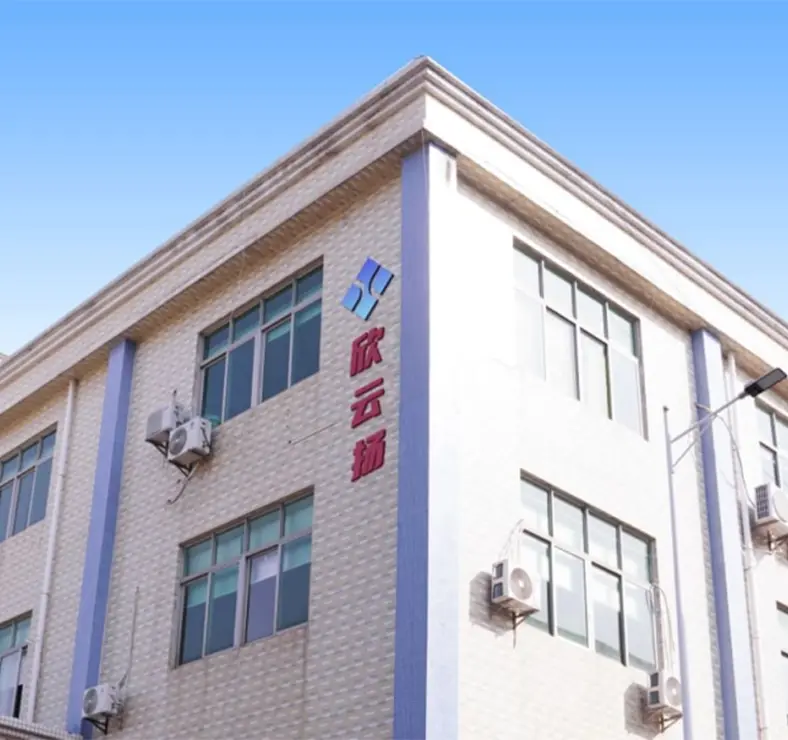
A transparent look into Xinyunyang's high-tech manufacturing facility. We deploy advanced progressive die stamping machines, state-of-the-art multi-axis CNC suites, and precision testing equipment.
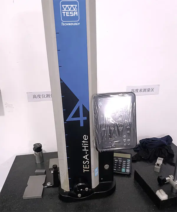
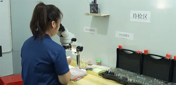
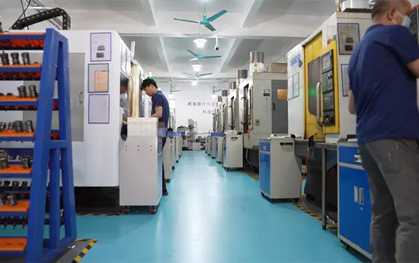
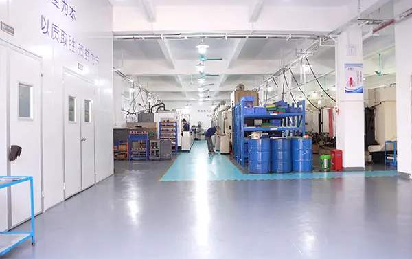
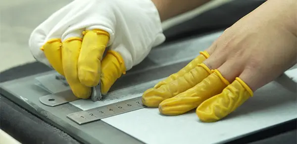
Explore professional, technical answers to critical engineering and procurement questions regarding Kovar stampings.
For standard Kovar stamping components (such as hermetic optical module covers or standard IC lids), tool design and initial samples are completed in 3 to 4 weeks. High-complexity deep-draw stampings requiring multi-stage progressive tooling typically require 5 to 6 weeks. Our integrated ISO 9001 scheduling and DFM systems routinely compress traditional development times by 15% to 20%.
To ensure pristine glass-to-metal sealing and gold-wire bonding compatibility, stamped Kovar parts are treated via professional vacuum or hydrogen-atmosphere cleaning cycles, followed by high-purity electro-plating. We offer multi-layer plating, including nickel underplating (1.5–3.0 μm) and pure gold overplating (typically 0.5–1.5 μm) according to MIL-G-45204 standards, preventing oxidation and guaranteeing excellent solderability.
Yes. We possess dedicated CNC rapid prototyping cells and wire-EDM processing systems specifically configured for low-volume engineering trial runs. This allows you to evaluate design performance and thermal curves prior to investing in dedicated progressive hard tooling.
Flatness is highly critical to avoid leaks during subsequent seam-welding or laser welding processes. We utilize customized double-disc grinding and high-precision flattening die systems built directly into the stamping run, routinely holding flatness tolerances within ≤0.05mm across the entire sealing perimeter.
 Xinyunyang Precision